VLSI BASED TRAININGS 2025
8 Weeks Project based Analog Circuit Design training
Current students of B.E./B.Tech/B.Sc/M.Tech/M.S/M.Sc in Electronics/Electrical/Instrumentation
Fees: 6,999/- 4,999/-
Mode: Online Daily Live Sessions.
Connect with us for detailed syllabus and other details
10 Weeks Project based Analog Circuit Design training for Professionals
Any Working Professional who wants to gain additional knowledge in Circuit Design.
Fees: 15,999/- 12,999/-
Mode: Online Daily Live Sessions.
Connect with us for detailed syllabus and other details
8 Weeks Project based Verilog Design training
Current students of B.E./B.Tech/B.Sc/M.Tech/M.S/M.Sc in Electronics/Electrical/Instrumentation
Fees: 6,999/- 4,999/-
Mode: Online Daily Live Sessions.
Connect with us for detailed syllabus and other details

8 Weeks Project based Web Development training
Current students of B.E./B.Tech/B.Sc/M.Tech/M.S/M.Sc in Electronics/Electrical/Instrumentation
Fees: 6,999/- 4,999/-Mode: Online Daily Live Sessions.
Connect with us for detailed syllabus and other details
9 Weeks Project based Analog & Digital Electronics training
Current 1st/2nd year students of B.E./B.Tech/B.Sc in any engineering branch
Fees: 12,999/- 9,999/-
Mode: Online Daily Live Sessions.
Connect with us for detailed syllabus and other details

8 Weeks Project based IoT training
Current students of B.E./B.Tech/B.Sc/M.Tech/M.S/M.Sc
Fees: 6,999/- 4,999/-Mode: Online Daily Live Sessions.
Connect with us for detailed syllabus and other details
"Discovering basICs"
Blended mode Training & Internship program in the domains of
VLSI, IoT, and Generative AI
A unique Opportunity to all the final year & pre final Engineering students to learn the concepts of Analog IC design, IoT, Generative AI with a major project.
Join Our “PROJECT BASED TRAINING” On “ANALOG IC Design”
Complete your academic project with proper training & guidance from industry expert and come up with wonderful industry relevant final year project.
Live Online Sessions.
What will you learn
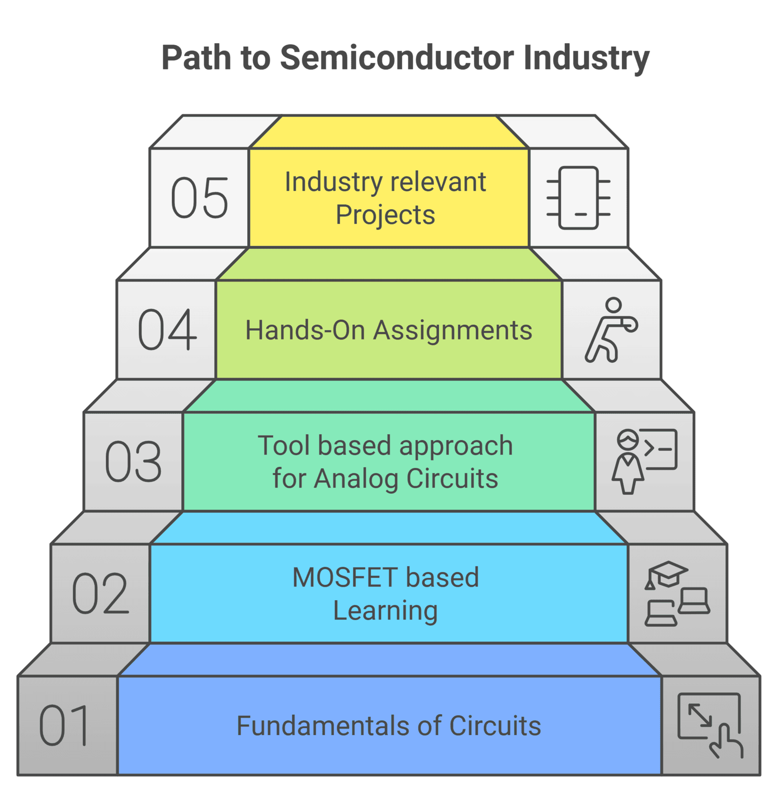
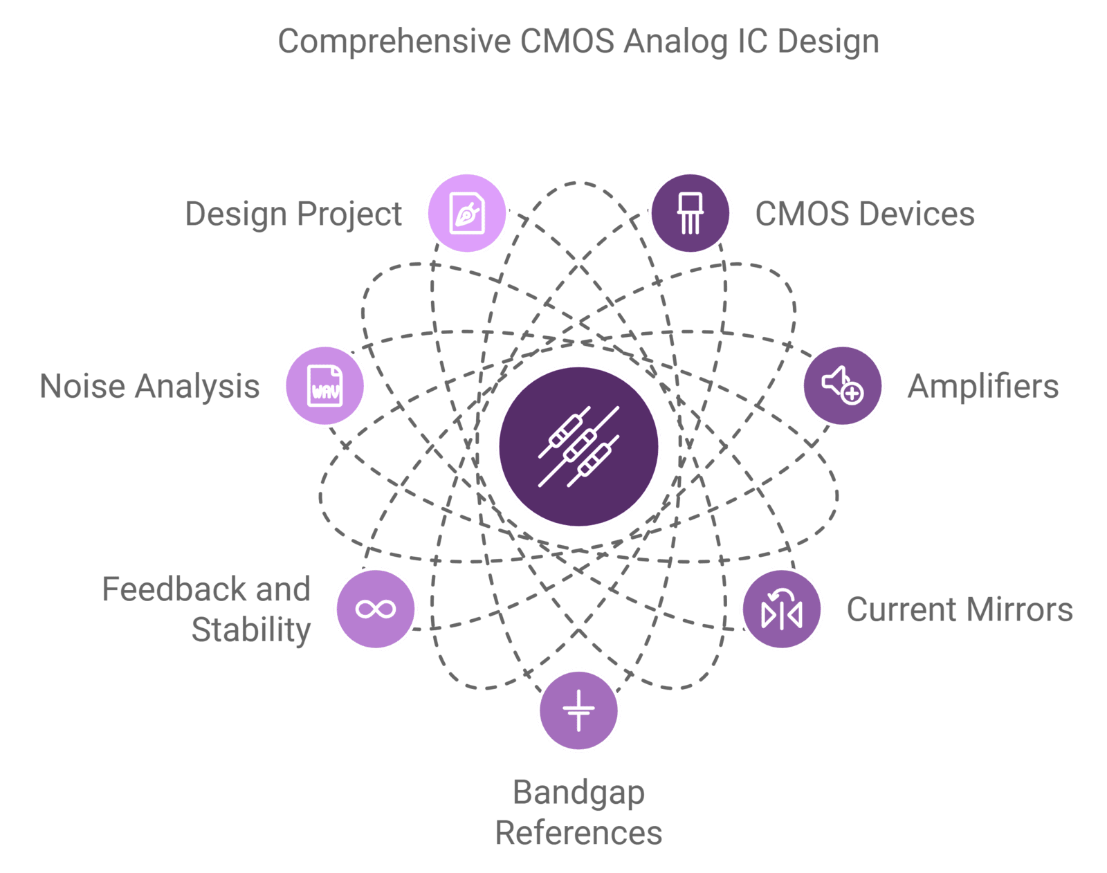
All the Training/Internship covers the design of CMOS analog integrated circuits with a focus on theoretical and practical circuit analysis, as well as design techniques from system functional blocks and transistor-level device physics. Fundamental concepts include CMOS devices emphasizing functionality limitations caused by short channel effects, single stage amplifiers, current mirrors, bandgap references, differential amplifiers, and operational amplifier. Building upon these concepts, the course explores multi-stage amplifiers, feedback, frequency response, stability, frequency compensation and noise analysis. Design of analog ICs of small to medium complexity and verifying them using simulation tools. Special emphasis is made throughout the course on understanding the effects of device parasitic and on developing device physics-driven circuit analysis and design skills. The course concludes with a design project.
4 Months Intensive Job oriented Training on Analog Design
For Details, Please contact us at 7019069046 or email your query to admin@sakshamsemiconductors.com
Course Overview
This course covers the design of CMOS analog integrated circuits with a focus on theoretical and practical circuit analysis, as well as design techniques from system functional blocks and transistor-level device physics. Fundamental concepts include CMOS devices emphasizing functionality limitations caused by short channel effects, single stage amplifiers, current mirrors, bandgap references, differential amplifiers, and operational amplifier. Building upon these concepts, the course explores multi-stage amplifiers, feedback, frequency response, stability, frequency compensation and noise analysis. Design of analog ICs of small to medium complexity and verifying them using simulation tools. Special emphasis is made throughout the course on understanding the effects of device parasitic and on developing device physics-driven circuit analysis and design skills. The course concludes with a design project.
Course Delivery
- Live Online Sessions daily 1 hours.
- Module specific Lecture sessions and hands on session on the go with assignments to monitor the progress.
- Continuous support extended through WhatsApp on the go.
Qualification:
- B.E. / B.Tech in Electronics / Electrical / Instrumentation
- M.Tech / M.S in VLSI / Embedded Systems / Electronics / Similar
Who Can attend this course
- College fresher with a passion towards Analog Circuit design, and willing to explore opportunities in the VLSI Industry.
- Professionals Working in VLSI industry, with some insights on MOS circuits and willing to switch to Analog Circuit design.
- Working professional from other VLSI domain and would like to switch to circuit design.
- Working professional who wants to strengthen circuit design concepts.
- Any Engineering Faculty from Electronics department who would like to get practical exposure to Analog circuit design.
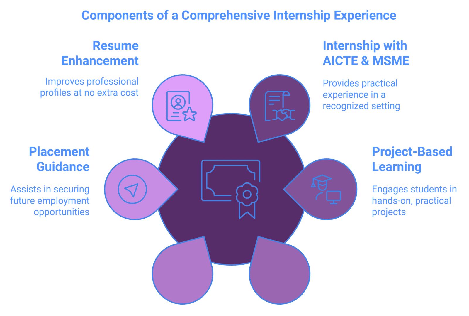
Technical Support extended until placed
Comprehensive Placement Assistance including resume preparation, Mock Interviews, LinkedIn Networking.
Works assigned, based on Industry Standard projects
Contents Covered in the Analog Design Training
1 Basic MOS Device Physics
1.1 MOFET Structure
1.2 MOS I/V Characteristics
1.2.1 Threshold Voltage
1.2.2 Derivation of I/V Characteristics
1.2.3 MOS Transconductance
1.3 Second-Order Effects
1.4 MOS Device Models
1.4.1 MOS Device Capacitances
1.4.2 MOS Small-Signal Model
1.4.3 NMOS Versus PMOS Devices
1.4.4 Long-Channel Versus Short-Channel Devices
2 Single-Stage Amplifiers
2.1 Applications
2.2 Common-Source Stage
2.2.1 Common-Source Stage with Resistive Load
2.2.2 CS Stage with Diode-Connected & Current-Source Load
2.2.3 CS Stage with Active Load
2.2.4 CS Stage with Triode Load
2.2.5 CS Stage with Source Degeneration
2.3 Source Follower
2.4 Common-Gate Stage
2.5 Cascode Stage
3 Differential Amplifiers
3.1 Single-Ended and Differential Operation
3.2 Basic Differential Pair
3.3 Common-Mode Response
3.4 Differential Pair with MOS Loads & Gilbert Cell
4 Current Mirrors and Biasing Techniques
4.1 Basic Current Mirrors
4.2 Cascode Current Mirrors
4.3 Active Current Mirrors - Large-Signal / Small-Signal Analysis
4.4 Biasing Techniques
4.4.1 CS Biasing & CG Biasing
4.4.2 Source Follower Biasing
4.4.3 Differential Pair Biasing
5 Frequency Response
5.1 RC Filters – Basics, Frequency Response and Bandwidth
5.2 Gain and Bandwidth, Gain and Phase Margin, why do we want good stability
5.3 Amplifiers in Series (Cascade Amp), Freq Response
6 Operational Amplifiers
6.1 General Considerations
6.1.1 Performance Parameters
6.2 One-Stage Op Amps
6.2.1 Basic Topologies
6.2.2 Design Procedure & Linear Scaling
6.2.3 Folded-Cascode Op Amps & Design Procedure
6.3 Two-Stage Op Amps
6.3.1 Design Procedure
6.4 Gain Boosting
6.4.1 Basic Idea
6.4.2 Circuit Implementation & Frequency Response
6.5 Output Swing Calculations & Common-Mode Feedback
6.6 Input Range Limitations & Slew Rate
6.7 Designing OpAmp- 1st Stage, 2nd stage, 2nd stage adding Miller Compensation
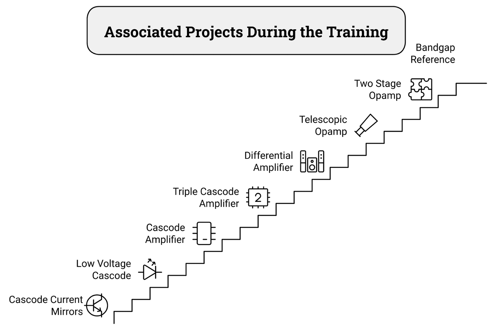
7 Reference Generator and Bandgap Reference circuit
7.1 Current Generator circuit, Independent Current Generator circuit
7.2. Bandgap Reference Circuit: Requirement of Voltage Reference, Voltage
Temperature Dependency, Diode as Voltage Reference, PTAT and CTAT Circuit,
PTAT Voltage Reference, PTAT with Current Mirror, Reference Voltage
Generation, Adding PTAT and CTAT, Vref Circuit, Voltage Reference α calculation
8 Analog Comparator
8.1 What is Analog Comparator? Application Areas
8.2 Specifications of Comparator
8.3 Parameters of Comparator
8.4 Two stage OpAmp as Comparator
8.5 Opamp as Comparator
8.6 Comparator with Inverter Output
8.7 Advanced features of comparator-Offset and offset cancellation, Offset
cancellation Scheme, Comparator with Hysteresis, Latched comparator or
comparator with Latch
9 Ring Oscillator
9.1 Oscillator Basics
9.2 3 Stage Oscillator – Ring Oscillator
9.3 Ring Oscillator Using Digital Inverters
9.4 Propagation delay of Inverter
9.5 Limitations of Inverter based Ring Oscillator
9.6 Differential Delay cell-based RO
9.7 Designing differential delay cell
10 IPs using Analog Building Blocks
10.1 Phase Locked Loop: What is PLL? Block Diagram, PLL as Frequency Multiplier,
Building Blocks of PLL, PFD + CP, Parameters of PLL
10.2 Digital to Analog Converter: What is a DAC? Binary Weighted Resistor, R-2R
Ladder, Advanced DAC: Current Steering DAC
10.3 LDOs
Assignments During the Course
Optimization of PMOS Width.
Nmos Characterization.
Transconductance gm, small signal output impedance (ro).
Various Nmos Configurations Output Impedance Rout.
ADE Assembler/MAESTRO For Multiple Test Bench Setup.
MONTE CARLO Analysis.
2x1 CMOS Multiplexer.
4x1 Multiplexer Using 2x1 Multiplexer.
8-Bit Carry Select Adder Using Hybrid Full Adder.
CMOS Inverter - DC & Transient Analysis.
NMOS | PMOS || Power Dissipation Calculation.
Create Array of Inverters.
Process Corner Analysis of CMOS Inverter.
CMOS Inverter || Parasitic Extraction and Post-Layout Simulation.
Inverter Delay Calculation.
Gate Sizing.
NAND gate Simulation (2 i/p and 3 i/p).
Calculation of Nmos Length L for Current Source.
Basic Current Mirror.
Cascode Current Mirror.
Low Voltage Cascode Current Mirror.
Common Source Amplifier.
Common Source Amplifier Nmos Diode connected Load.
CS Amplifier with current source load using PDM.
Casocde CS Amplifier with current source load using PDM.
Triple Casocde CS Amplifier with current source load using PDM.
Differential Amplifier with active load using PDM.
Differential Amplifier.
Op-amp.
Design of Telescopic Opamp using PDM.
ADVANCED CONCEPTS
SRAM Cell Stacking Transistor's to reduce Power Consumption.
TOOL BASED SKILL (CADENCE)
Cadence Graph Shortcuts Markers.
How to Use Piece Wise Linear (PWL/PWFL) Source in Cadence.
Export Simulation Graph data to Excel.
Advanced Options in Cadence.